-
E-mail
qeservice@enli.com.tw
-
Phone
18512186724
-
Address
Room 6C, Building 3, No. 100, Lane 1505, Zuchongzhi Road, Pudong New Area, Shanghai
Product Categories
Guangyan Technology Co., Ltd
How much does the optical sensor wafer tester cost
NegotiableUpdate on 01/16
- Model
- Nature of the Manufacturer
- Producers
- Product Category
- Place of Origin
Overview
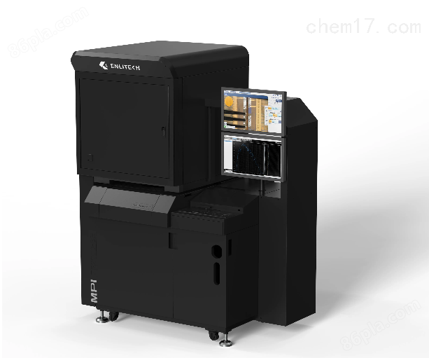
SG-O is a CIS/ALS/Light Sensor wafer tester that combines a highly uniform light source and a semi-automatic wafer detector. A highly uniform light source can provide a continuous white light spectrum from 400nm to 1700nm, as well as monochromatic light output with a certain FWHM at many different wavelengths. The detector can handle it. 200mm wafer size and single chip size greater than 1cm x 1cm. SG-O integrates an ultra-low noise thermal chuck that provides a temperature range of -60 ° C to 180 ° C
Product Details

feature
Highly uniform light source
Programmable automatic detector
Wide temperature and low noise chuck
application
CIS/ALS/Optical Sensor Wafer Testing
CIS/ALS/Optical Sensor Wafer Mapping and Yield Inspection
ToF sensor testing
Lidar sensor testing
InGaAs PD testing
SPAD sensor testing
Optical sensor simulation parameter testing:
quantum efficiency
spectral response
System gain
sensitivity
dynamic range
Dark current/noise
signal-to-noise ratio
Saturated capacity
Linear Error (LE)
DCNU (dark current non-uniformity)
PRNU (Light Response Non Uniformity)
System Design
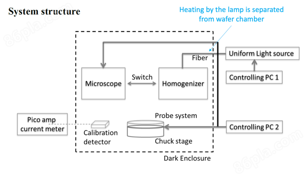
SG-O CIS/ALS/Light Sensor Tester (wafer level) system diagram. The highly uniform light source is controlled by PC-1. The light output is guided by optical fibers to an optical homogenizer to generate a uniform beam of light. The microscope and homogenizer are controlled by the automatic translation stage of PC-1 to switch positions and functions. The Probe system is MPI TS2000, controlled by PC-2. The position of the chuck table is also controlled by PC-2. The temperature of the hot card can be controlled between -55 ℃ and 180 ℃, covering most of the IC testing temperature range. The light intensity is detected and calibrated by a Si photodetector and an InGaAs photodetector using a picoampere ammeter.
Specifications
SG-O provides complete specifications for all the content you need in CIS/ALS/optical sensor wafer testing. The following are the main components and their detailed information. If you need more detailed information, please feel free to contact us at any time!
Highly uniform light source
10nm FWHM center wavelength:420nm,450nm,490nm,510nm,550nm,570nm,620nm,670nm,680nm,710nm, 780nm, 870nm
25nm FWHM center wavelength:1010nm,1250nm,1450nm
45 ± 5nm FWHM center wavelength: 815nm
Center wavelength of 50nm FWHM:1600nm
60 ± 5nm FWHM center wavelength:650nm
Center wavelength of 70 ± 5nm FWHM:485nm,555nm
Center wavelength of 100 ± 5nm FWHM:1600nm
Out of band transmittance ≤ 0.01%
Peak transmission in bandpass area ≥ 80%
Center wavelength tolerance: (a) ≤± 2nm; (b)~(g) ≤± 5nm
FWHM tolerance: (a) ≤± 2nm; (b)~(g) ≤± 5nm
Semi automatic wafer probe
Spectral radiometer
More specifications
SG-O integratedEnlitechAdvanced optical simulator technology and MPI automatic probe system.EnlitechProvide multiple optical options to meet users' requirements for CIS/ALS/optical sensor wafer testing, including wavelength range, light intensity, and uniform beam size. We have decades of experience in helping customers solve the challenges of CIS/ALS/optical sensor wafer testing and design changes. Please feel free to contact us for more detailed information. Our professional team will provide assistance to you!
main manifestations

Operating software for SG-O system. For highly uniform light source control software, SG-O provides light source system control and light intensity measurement. Provides Labview function palettes, driver/DLL files for various optical components. The software controls the translation stage to facilitate illumination on the equipment of the parts. The integration of integrated links includes sending/receiving commands, such as chip stepping, chip alignment/probing, etc.

CIS/ALS/Light Sensor Chip Images from SG-O Microscope System
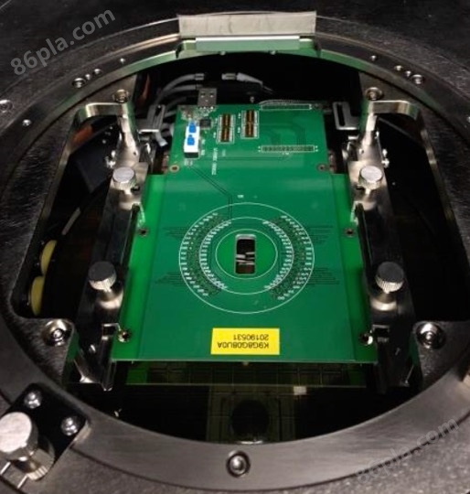

Installation diagram of probe card for CIS/ALS/Light Sensor wafer

Probe head image for CIS/ALS/optical sensor wafer inspection

The optical homogenizer of SG-O CIS wafer level tester

Optical simulation and performance of SG-O CIS wafer level tester optical homogenizer
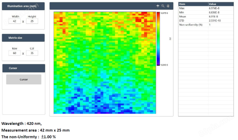
Beam uniformity, tested for beam spot uniformity using 42mm x 25mm at 420nm, with an non-uniformity of 1% as shown in the diagram
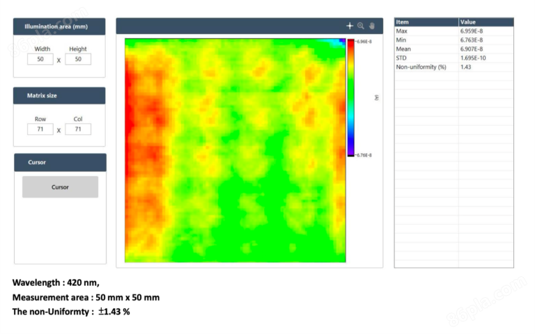
Beam uniformity, beam spot size of 50mm x 50mm, non-uniformity of 1.43% as shown in the diagram
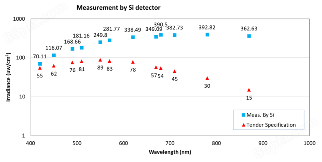
Monochromatic light intensity of different wavelengths, ranging from ultraviolet to near-infrared; The light intensity is measured by a Si radiometer, and the range of light intensity can be used for various CIS/ALS/light sensor testing diagrams

Monochromatic light intensity at different wavelengths from NIR to SWIR, measured by InGaAs radiometer as shown in the diagram
The highly uniform light source of SG-O has a super stable light engine, with short-term or long-term light intensity instability better than 0.2% across the entire wavelength range.

The diagram shows the short-term instability of light intensity tested under 420nm monochromatic light output. The light instability is monitored by a Si radiometer for 60 minutes, and the instability for 1 hour is 0.12%

The diagram shows the short-term instability of light intensity tested under 1250nm monochromatic light output. The light instability was monitored by a SInGaAs radiometer for 60 minutes, and the instability after 1 hour was 0.09%
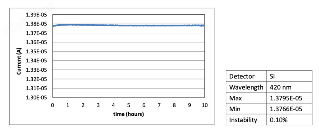
Short term instability of light intensity was tested under 420nm monochromatic light output. The light instability was monitored by a Si radiometer for 10 hours, and the instability after 10 hours was 0.1% as shown in the diagram
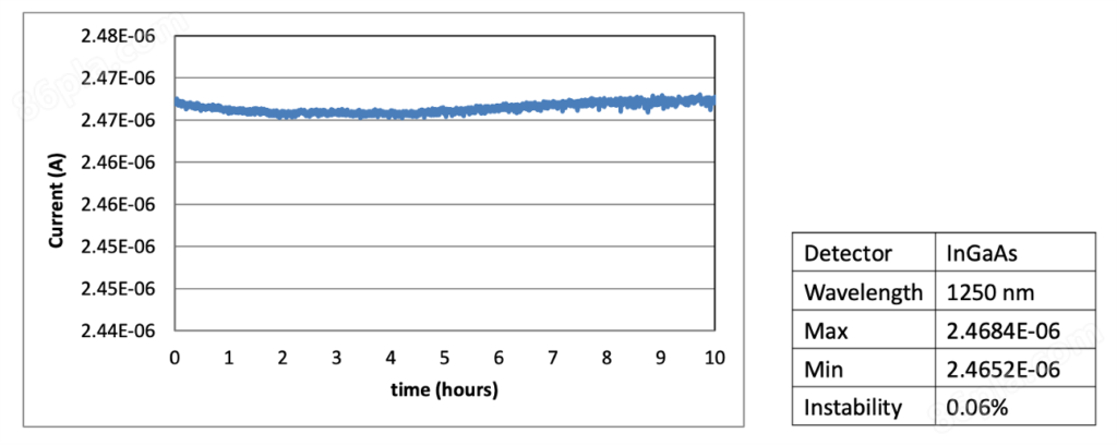
Short term instability of light intensity was tested under 1250nm monochromatic light output. The light instability was monitored by a SInGaAs radiometer for 10 hours, and the 10 hour instability was 0.06% as shown in the diagram
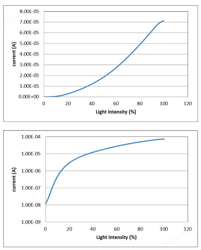
The diagram shows the light intensity attenuator of the SG-O system, and the light output intensity can be controlled by a PC with a resolution of at least 1000 steps

Information manual for automatic detectors,SG-O CIS / ALS / Light-SensorThe wafer tester is integratedMPIProbe, more details can be found inMPIFound on the website
data source MPI
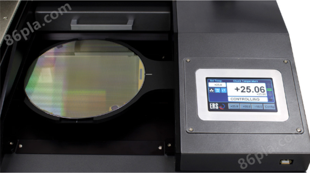
The SG-O probe system is equipped with an automatic single-chip loader. Easy to load CIS/ALS/Light Sensor wafers. Loading and unloading wafers is direct and intuitive for users. The front of the feeding room also integrates a temperature control panel for easy operation.
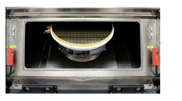
The SG-O CIS/ALS/Light Sensor wafer tester also has a manual loading function, which can manually load wafers from the front door. The front door has a safety management function that can automatically monitor the temperature of the chuck and prevent the door from opening during testing to protect the safety of CIS/ALS/Light Sensor wafers and users.
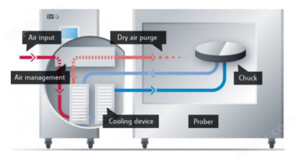
The thermal chuck of SG-O CIS/ALS/Light Sensor wafer tester is temperature controlled by the CDA system minimized by ERS, which is more efficient than before. The temperature range can cover -80 ° C to 180 ° C (depending on ERA's model). Nitrogen purging can be carried out by using a separate valve. For CIS/ALS/optical sensor wafer testing, the target temperature rise rate and stability are excellent, and can be used in any
Under certain conditions (such as space).
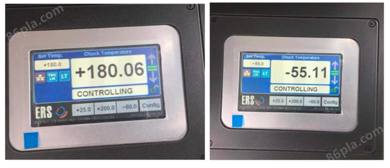
The probe card size capability can range from 4.5 inches to 8 inches in length, as shown in the figure for DUT and SG-O high uniformity light sourcethe latterThe working distance of an optical component exceeds 200mm

The probe card size capability can range from 4.5 inches to 8 inches in length, as shown in the figure for DUT and SG-O high uniformity light sourcethe latterThe working distance of an optical component exceeds 200mm
Similar Product Recommend