


09,17,2026 5 views
The global AI computing hardware continues to iterate and expand, and high-speed optical interconnection, as the core hardware base for computing power transmission, is experiencing explosive growth. The upgrade of computing power drives the acceleration of mass production and landing of 800G and 1.6T high-speed optical modules. Goldman Sachs predicts that the global optical module market size will reach approximately $67.7 billion from 2026 to 2028.
The optical chip is the "heart" of the optical module, responsible for the conversion of electro-optical signals; Its cost proportion in devices has rapidly increased from 40% -50%, and high-end products are expected to exceed 70%. The performance and stability of optical modules depend on the quality of the underlying optical chips. For a long time, the domestic production and testing equipment for optical chips has been highly dependent on imports, with pain points such as high technical barriers, high procurement costs, and long delivery cycles. This bottleneck has constrained the large-scale production process of domestically produced high-speed optical devices.
At the CIOE2026 China International Optoelectronics Expo, Tuosida's joint venture company Laile Optoelectronics brings a new solution——CHIP TEST chip testing system makes its first public appearanceOnce exhibited, it became the focus of the booth,Received key attention from numerous industry chain merchants and investment institutions.
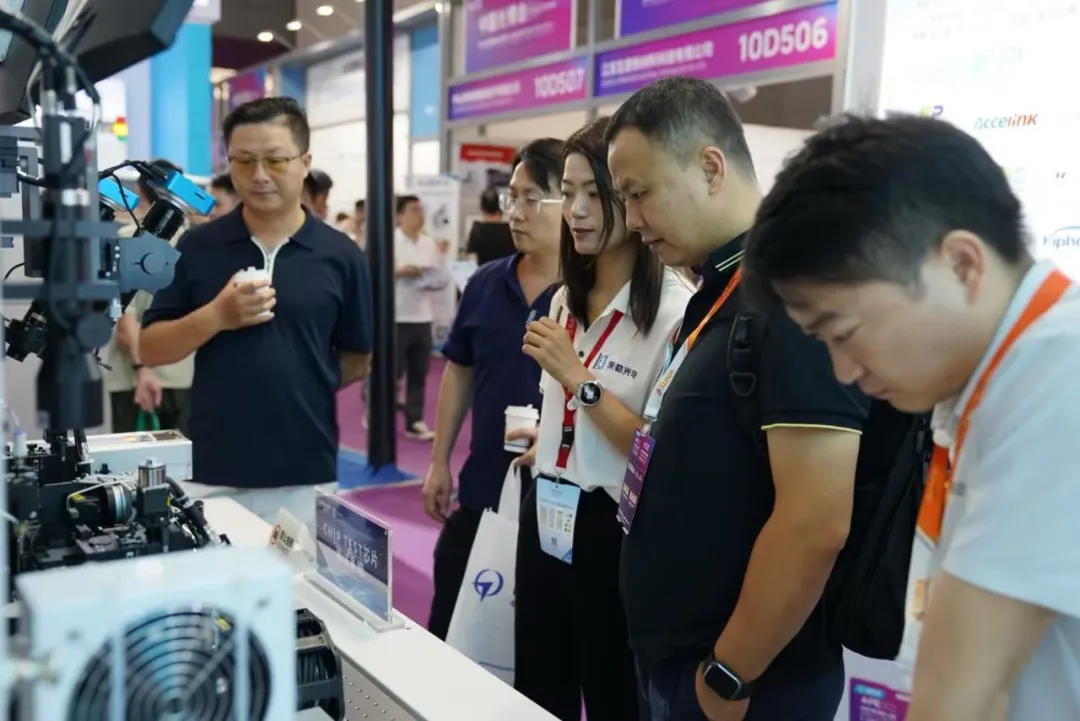
The all-new heavyweight debut this timeCHIP TEST chip testing system is specially designed by Laile Optoelectronics for mass production testing of laser chipsThe device can complete comprehensive data detection of chip optoelectronic performance, spectrum, divergence angle, etc. in one stop, automatically generate standard test reports, and adapt to mainstream chip categories such as DFB and EML.Accurately screen out defective chips from the source, significantly improve backend packaging yield, and reduce production costs,Truly supplement the full chain capability of domestic optical devices with "chip detection+automatic coupling".

In addition to new products, Laile Optoelectronics' mature main equipment is exhibited simultaneously, covering the entire process of optical device production, including dual FA automatic coupling system and Pump laser automatic coupling system. Relying on micro nano precision multi axis motion platform and self-developed optical coupling algorithm, the equipment achieves fully automatic optical path optimization alignment, eliminating manual repeated debugging, adapting to the new process of 800G/1.6T high-speed optical devices for mass production, and matching the production needs of the AI computing power industry for rapid expansion.

Dual FA automatic coupling system

Pump Laser Fully Automatic Coupling System
The current demand for high-speed optical devices continues to explode, and high-end detection and coupling equipment generally face tight production capacity and high delivery pressure. Relying on Topstar's mature large-scale manufacturing capabilities and supply chain system, it can help Laile Optoelectronics solve industry delivery pain points. Both parties can also integrate product capabilities, launch an integrated optical communication line solution, adapt to high-end optical manufacturing production needs, and expand market space in both directions.
By laying out high-end equipment for manufacturing AI hardware upwards, delving deeper into data capabilities and industrial vertical models downwards, and implementing tailored intelligent products, Tuosida will provide customers with more suitable intelligent manufacturing solutions, helping them solve production pain points and opening up new growth space for the long-term growth of the enterprise itself.
Writing | Xu Jingyu
Review | Laile Optoelectronics
Image source | Tuosida


